Researchers from the Technion have developed a smart light source based on a single atomic layer of matter. The achievement will enable the development of new quantum applications in the field of computing and other fields
Researchers at the Technion have developed a new light source based on a single atomic layer. The innovative development, published in the journal Nature Nanotechnology, Allows control ofSpin Of the photons emitted in a two-dimensional material and paving the way for new photonic devices based on “atomic scale spin optics”. The discovery is based on the interaction of a single atomic layer with nano-antenna arrays on a silicon chip while creating defects in photonic crystals.
The study was conducted in the study group of Prof. Erez Hasman, Head of the Photonics Laboratory on an Atomic Scale, with Prof. Elad Koren, Head of the Laboratory for Electronic Nanomaterials and Nanocomponents in the Faculty of Materials Science and Engineering. The two research groups belong to the Helen Diller Quantum Center and the Russell Berry Institute of Nanotechnology. The study was conducted and led by Dr. Kexiu Rong and Dr. Bo Wang in collaboration with researchers Dr. Elhanan Magid, Dr. Vladimir Kleiner, Avi Reuven, Bar Cohen and Shaul Katzenelson.
What are two-dimensional materials? According to Prof. Koren, “In 2004, the possibility of forming a single atomic layer was first examined when physicists Andre Game and Konstantin Novoslov, later Nobel laureates in physics (2010), developed a simple method of forming single layers of carbon atoms. Another layer until a single atomic layer called graphene is obtained.They show that the atomic material layer is very different in properties from the properties of the material in its three-dimensional form.It is a material 100 times stronger than steel and has extraordinary electrical properties, and is estimated to revolutionize “In monitors and screens, in solar cells, etc.” Following this discovery, atomic layers were developed from other materials, and they also exhibited surprising and unique properties. “
Prof. Hasman goes on to explain: “Following the discovery of graphene, many two-dimensional materials have been discovered and studied, such as various semiconductors that also allow interesting optical properties. Standard electronic chips are based on silicon, which severely limits the development of next-generation computers Among other things, due to the lack of a vital state called ‘direct energy gap’ in silicon. Of the chips. “
To minimize the electronic chip and significantly increase the speed of processing and the rate of information transfer, the currently accepted approach is spintronics – performing operations on the spin, one of the important properties of the electron, and not on the current of the electrons. A few years ago, Prof. Erez Hasman of the Technion established a new field called Spinaoptics, Which makes it possible to utilize the spin of the photons using meta-surfaces for the benefit of transmitting and processing information in photonic chips. The transfer of information is based on the control of the photonic spin with the help of nanopotonics – optics at the nanometer scale.
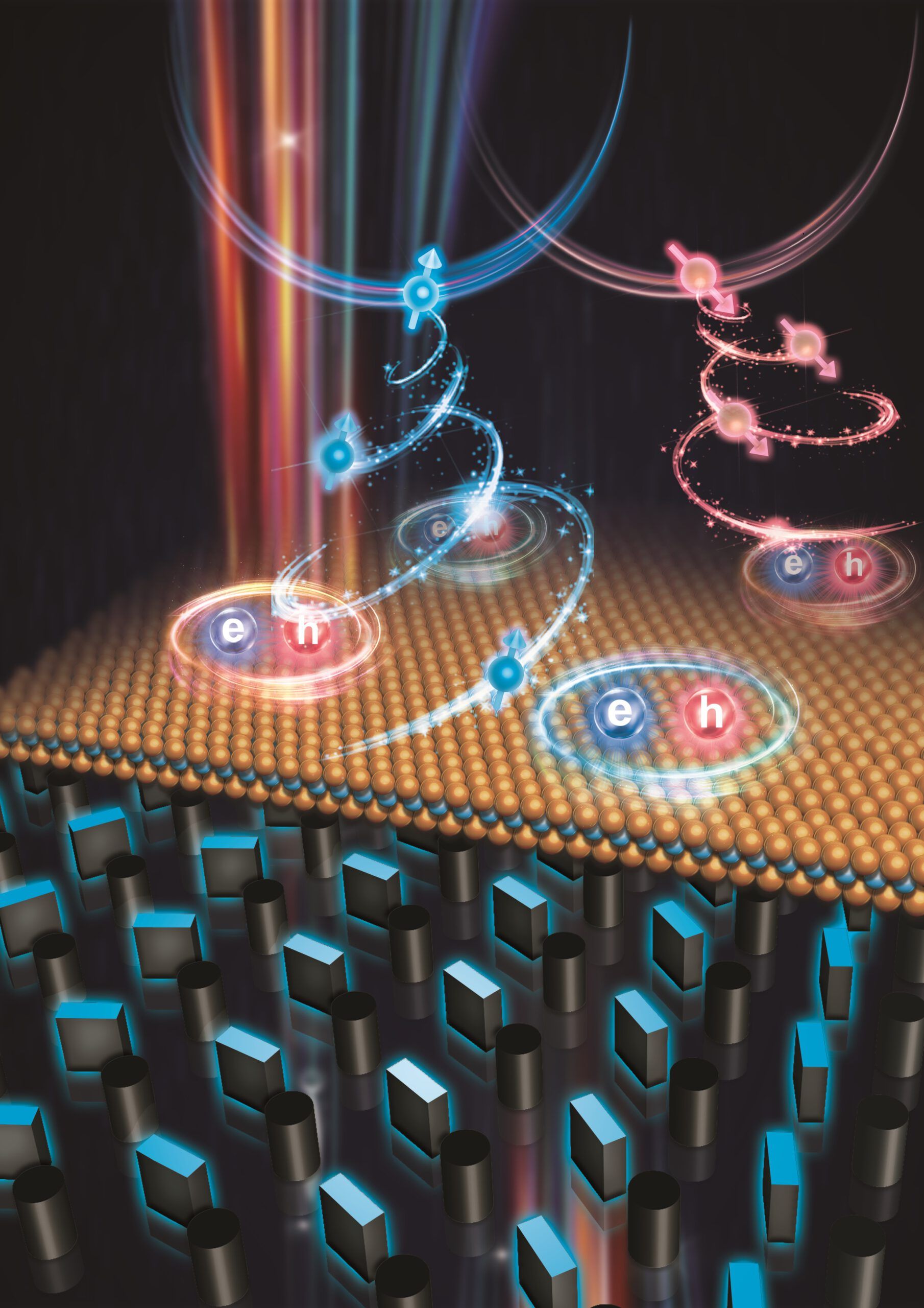
Two-dimensional semiconductor materials are characterized by energy levels whose emission depends on spin valleys, due to the breaking of the symmetry of the mirror. Technion researchers have decided to take advantage of this feature and pair a single atomic layer of tungsten selenium (WSe2 Lanopotonics – Nanowantons that allow symmetry to be broken in the photonic spin and receive a chip on an atomic scale that allows a light source and photonic devices while controlling and processing information in the photonic spin.
The researchers created a two-dimensional crystalline structure from silicon that creates an energy gap in the emission domain of the two-dimensional material so that the atomic semiconductor coupling to the photonic crystal blocks all optical emission channels from the two-dimensional material. By creating smart defects within the photonic crystal, controlling the phase of the defects with their geometry and coupling them, the researchers created a light source from a single atomic layer that separates and sorts the spins of the photons emitted from the two-dimensional semiconductor. This scientific discovery will make it possible to combine spintronics and spin optics to develop a wide range of devices on an atomic scale.
Prof. Hasman proudly notes that “this prestigious publication shows the importance of multidisciplinary research that combines physics, chemistry, materials science and engineering.”
The study was supported by the National Science Foundation (ISF), the Department of Science and Technology, the Technion and the U.S. Air Force Research Bureau. The components were implemented at the Sarah and Moshe Zisapel Nanoelectronics Center (MNFU) at the Technion.
Laboratory sites: https://hasman.technion.ac.il/ https://koren.net.technion.ac.il/
For an article in Nature Nanotechnology click here
More on the subject on the Yadan website:
These were the details of the news Spine optics on an atomic scale: the chips of the future for this day. We hope that we have succeeded by giving you the full details and information. To follow all our news, you can subscribe to the alerts system or to one of our different systems to provide you with all that is new.
It is also worth noting that the original news has been published and is available at news1.news and the editorial team at AlKhaleej Today has confirmed it and it has been modified, and it may have been completely transferred or quoted from it and you can read and follow this news from its main source.