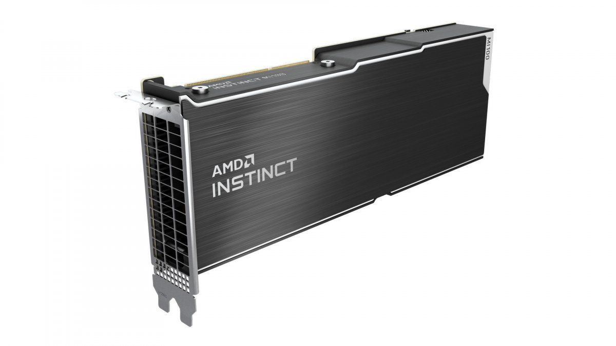


The AMD Instinct MI100 is the first compute accelerator card with the new CDNA architecture and is produced using 7 nanometer technology at TSMC. AMD wants to compete with Nvidia’s A100 with the PCIe 4.0 card and its 32 GByte HBM2 memory and has not only revised the compute units known from the GCN architecture, but has also built significantly more of them into the chip. The card is to be had for system integrators from 6400 US dollars and thus clearly undercuts Nvidia’s A100 PCIe version, which is available from 10,700 euros.
A lot of flops, a lot of honor
When it comes to technical specifications, AMD is once again cracking it – probably also to put competitor Nvidia in its place with the A100 accelerator in some areas.
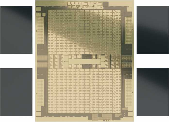
The CDNA chip “Arcturus” has 120 active compute units (CUs) on the MI100 and even if AMD confirmed on request that this was the full expansion, images of the chip suggest that there are 8 more CUs. We asked AMD again for clarification and are currently awaiting the answer.
AMD Instinct MI100 block diagram
(Image: AMD)
As with the closely related graphics chips with GCN architecture (GraphicsCore Next), the 120 CUs each have 64 shader processing cores, which results in 7680 ALUs for the entire chip. Together with a maximum boost clock rate of 1502 MHz, this results in a throughput of 23.07 TFlops with single accuracy (FP32). As befits an HPC accelerator, the FP64 rate is half, i.e. 11.5 TFlops – and thus not only above the 10 TFlops mark but also around 19 percent above the comparable value of Nvidia’s A100 accelerator in SXM4 format.
Arcturus-Die-Shot: CDNA accelerator with 120 active compute units and four HBM2 stacks
(Image: AMD)
As with the MI50 / MI60, the rake beast is fed by four HBM2 stacks. These each hold 8 GB and are clocked at 1200 MHz, which is good for a transfer rate of 1.228 TB / s. An 8 MByte level 2 cache (6 TByte / s) is supposed to cushion the memory access. From the registers to the HBM2, everything is secured by ECC (SECDED).
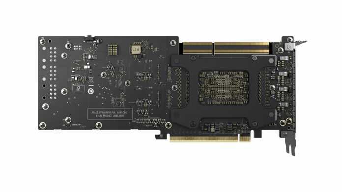
In addition to PCI-Express 4.0, each MI100 card has three Infinity links at 92 GByte / s – a total of 276 GByte / s. This means that directly networked groups of four MI100s are now possible, which can form a coherent memory area.
Matrix Core Engines: A bit of a tensor
The compute units of the MI100 are similar to those of the previous generation Graphics Core Next, but have been further upgraded by AMD for compute use. In order to achieve a higher throughput with matrix-matrix multiplications, AMD has expanded the circuits and register ports and calls the result the Matrix Core Engine.
AMD has chosen a different path than Nvidia with their tensor cores. The Core Matrix Engines work consistently with full FP32 accuracy. On the other hand, their maximum throughput is lower and they are not suitable for FP64 calculations. Therefore, it is difficult to compare the maximum throughput between the two approaches. Those who consistently rely on full FP32 accuracy will do better with AMD. Those who can also use the alternative TF32 or lower accuracy will benefit from the Nvidia accelerators.
Both approaches have in common that they support the BFloat16 (BF16) format, which combines the value range of FP32 (8-bit exponent) with the accuracy of FP16 (7-bit mantissa, plus 1 sign bit) and is known as de facto has established an alternative to full FP32 in AI training. In the CDNA whitepaper for BFloat16, however, AMD specifies 10 bit mantissa and 5 bit exponent, which actually corresponds to FP16.
| Instinct MI100 (PCIe) | A100 (SXM) | Tesla V100 | Tesla P100 | |
| Manufacturer | AMD | Nvidia | Nvidia | Nvidia |
| GPU | CDNA Arcturus | A100 (Ampere) | GV100 (Vault) | GP100 (Pascal) |
| CUs/SMs | 120 | 108 | 80 | 56 |
| FP32 Cores / SM | 64 | 64 | 64 | 64 |
| FP32 Cores / GPU | 7680 | 6912 | 5120 | 3584 |
| FP64 Cores / SM | 32 | 32 | 32 | 32 |
| FP64 Cores / GPU | 3840 | 3456 | 2560 | 1792 |
| Matrix Multiply Engines / GPU | 480 | 432 | 640 | — |
| GPU Boost Clock | 1502 | k.A. | 1455 MHz | 1480 MHz |
| Peak FP32 / FP64 TFlops | 23,07 / 11,54 | 19,5 / 9,7 | 15 / 7,5 | 10,6 / 5,3 |
| Peak Tensor Core TFlops | — | 156 (TF32) / 312 (TF32 Structural Sparsity) | 120 (Mixed Precision) | — |
| Peak Matrix Core Engine TFlops | 46,1 (FP32) | — | — | — |
| Peak FP16 / BF16 TFlops | 184,6 / 92,3 | 312 / 312 (624 / 624 Structural Sparsity) | 125 / 125 | 21,1 / — |
| Peak INT8 / INT4 TOps | 184,6 / 184,6 | 624 / 1248 (1248 / 2496 Structural Sparsity) | 62 / — | 21,1 / — |
| Memory interface | 4096 Bit HBM2 | 5120 Bit HBM2 | 4096 Bit HBM2 | 4096 Bit HBM2 |
| Memory size | 32 GByte | 40 GByte | 16 GByte | 16 GByte |
| Memory transfer rate | 1,2 TByte/s | 1,55 TByte/s | 0,9 TByte/s | 0,73 TByte/s |
| TDP | 300 Watt | 400 Watt (SXM) | 300 Watt | 300 Watt |
| Transistors (billion) | k.A. | 54 billion | 21.1 billion | 15.3 billion |
| GPU Die Size | k.A. | 826 mm² | 815 mm² | 610 mm² |
| production | 7 nm | 7 nm | 12 nm FFN | 16 nm FinFET+ |
AMD Instinct MI100 with complex IF connection and soldering points for up to three eight-pole connections.
(Image: AMD)
Without Radeon, without displays
After Nvidia’s Tesla and Quadro waiver, AMD is now also changing the branding of the accelerator cards and removing the Radeon from the product name. The card is only called AMD Instinct MI100 – although the number, unlike earlier Instinct cards, no longer stands for the FP16 processing power.
In order to accommodate as much computing power as possible in the TDP range of 300 watts, AMD has, according to its own information, omitted many hardwired functions that are necessary for a graphics card in the first CDNA chip “Arcturus”. This includes the rasterization units, tesselator hardware, special graphics buffers, the blending units in the raster output stages and the display engine. The MI100 cannot be used as a graphics card and Crysis does not run on it either.
However, AMD has not removed the video engines, i.e. the specialized decoders and encoders. Reason: Machine learning is often used to analyze video streams or image recognition.
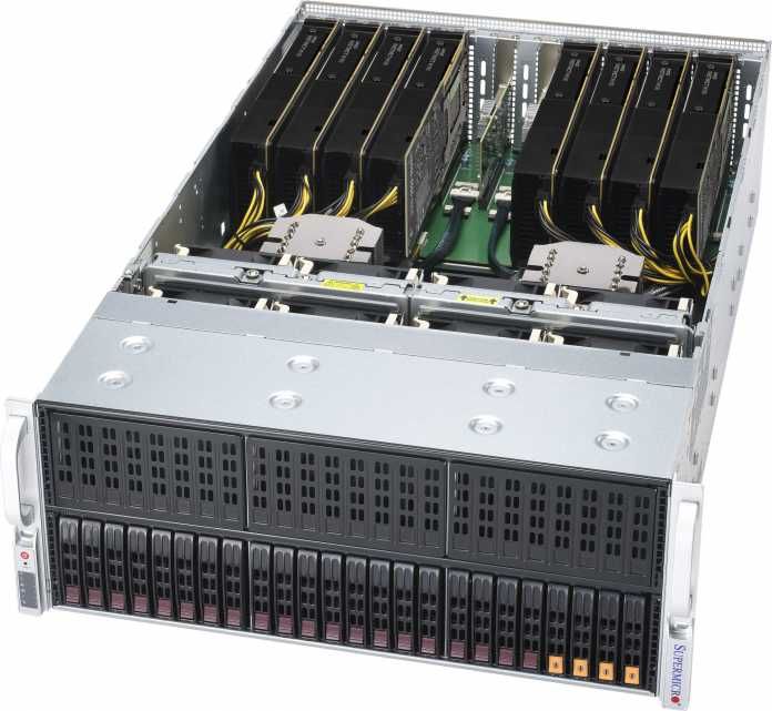
One of the first rack servers comes from Supermicro (Dell, HPE and Gigabyte also have similar products in their range). With the real cards it is noticeable that only an eight-pin connector is sufficient.
(Bild: AMD/Supermicro)
(csp)
*We just want readers to access information more quickly and easily with other multilingual content, instead of information only available in a certain language.
*We always respect the copyright of the content of the author and always include the original link of the source article.If the author disagrees, just leave the report below the article, the article will be edited or deleted at the request of the author. Thanks very much! Best regards!
These were the details of the news Server accelerator AMD Instinct MI100: Without Radeon, but with 11.5 FP64... for this day. We hope that we have succeeded by giving you the full details and information. To follow all our news, you can subscribe to the alerts system or to one of our different systems to provide you with all that is new.
It is also worth noting that the original news has been published and is available at en24news and the editorial team at AlKhaleej Today has confirmed it and it has been modified, and it may have been completely transferred or quoted from it and you can read and follow this news from its main source.